Reverse Engineering PCB Insights for 2026 Canton Fair Buyers?
As we approach the 2026 Canton Fair, buyers seeking insights into Reverse Engineering Pcb technology must be prepared. This year’s event showcases advancements in electronics and manufacturing, making it essential for attendees to understand the complexities of PCB design. The fair spans over several phases, focusing on various sectors from advanced manufacturing to consumer goods.
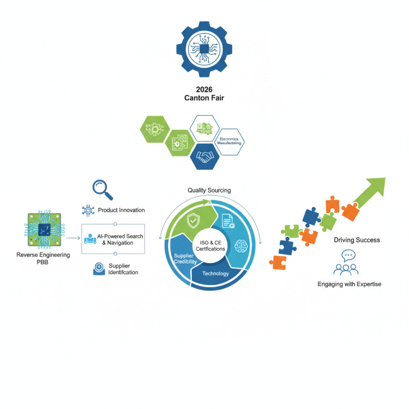
Reverse engineering PCB can unlock new pathways for product innovation. Buyers will encounter over 1.5 million square meters of exhibition space. Yet, navigating this vast area may prove challenging. The introduction of AI-powered search and navigation facilitates easier exploration. Still, buyers must continuously refine their strategies to identify the best suppliers.
A potential area of concern is ensuring quality in PCB sourcing. Certifications like ISO and CE remain crucial for evaluating suppliers. This aspect of Reverse Engineering PCB demands careful consideration. Striking a balance between technology and supplier credibility can often lead to missed opportunities. Engaging with the right expertise at the Canton Fair is vital for driving success.
Understanding PCB Reverse Engineering: Trends and Techniques for 2026 Buyers
As the 2026 Canton Fair approaches, reverse engineering of PCBs becomes crucial. This practice involves breaking down existing circuit boards to understand their design and functionality. Many buyers seek insights into the latest trends and techniques to enhance their product offerings.
Emerging trends in PCB reverse engineering include the use of advanced software tools. These tools help create accurate 3D models and simulate electrical performance. Additionally, buyers are increasingly interested in sustainability. They want to know how to recycle and repurpose materials from older PCBs. However, this process can be complex and requires proper training.
Another technique gaining traction is the use of artificial intelligence. AI can analyze PCB layouts and identify potential improvements. Yet, not everyone is comfortable with technology. Some buyers may find it challenging to adapt to these innovations. This gap in understanding often leads to missed opportunities. It's clear that gaining skilled insights into PCB designs requires both effort and investment.
Market Dynamics: The Growth of PCB Reverse Engineering in Electronics Industry
The electronics industry is experiencing significant shifts. A key trend is the growth of PCB reverse engineering. Recent reports highlight that the PCB market is expected to reach $83 billion by 2026, with reverse engineering playing a critical role. This surge reflects rising demand for innovation and rapid prototyping.
Companies seeking to enhance their designs utilize reverse engineering. This process not only aids in product analysis but also accelerates development timelines. According to a leading industry report, 45% of manufacturers have adopted reverse engineering techniques. It allows them to identify design flaws and optimize functionality. Still, the practice raises ethical questions.
One challenge is the balance between innovation and intellectual property rights. While companies strive for advancement, they must navigate the risks of infringement. The integration of reverse engineering into PCB development offers vast opportunities but requires careful consideration. The evolving market dynamics will force buyers to reevaluate their strategies while maintaining compliance with regulations.
Key Tools and Software for Effective PCB Reverse Engineering Processes
Reverse engineering PCB (printed circuit boards) is gaining traction among buyers at trade fairs, like the Canton Fair in 2026. Utilizing effective tools and software is essential for successful processes in this field. Computer-aided design (CAD) software is one cornerstone. It helps visualize the board layout and design. However, selecting the right CAD software can be challenging. Users often struggle with complex interfaces. Each tool has its own learning curve, which can be frustrating.
Another vital component is the use of a scanner. High-resolution scanners enable accurate image capture of PCBs. This ensures detail retention for analysis. Yet, not all scanners are created equal. Some may miss intricate details or produce low-quality images. It's advisable to test different devices to find the best fit.
Finally, data analysis tools play a crucial role in interpreting reversed designs. They help in understanding component functions and placements. Many users find that these tools can be overly complicated. The key is to familiarize yourself with the data outputs. This will enhance your proficiency and accuracy over time. Each tool and software choice should align with specific project needs. Ultimately, continuous learning and adaptation are necessary for mastering PCB reverse engineering.
Regulatory Considerations: Compliance and Best Practices for PCB Reverse Engineering
Reverse engineering PCBs offers valuable insights for buyers at the 2026 Canton Fair. However, navigating the regulatory landscape is crucial. Compliance with local and international regulations can be complex. Failing to adhere to these laws could lead to serious consequences. Each region has unique requirements. Understanding these can prevent costly mistakes.
Best practices are essential for successful reverse engineering. Establish clear documentation and ensure quality control throughout the process. Use proper tools and techniques to avoid damaging sensitive components. It's important to respect intellectual property rights. Ignoring these can result in legal issues. Additionally, ensure transparency in your methods. Share knowledge with your team to foster a culture of compliance.
Reflecting on the process can improve outcomes. Many companies overlook the importance of continuous learning. It’s key to regularly update your practices based on new regulations. Don’t underestimate the value of feedback. Engaging with peers helps in identifying potential pitfalls. Always question your methods for improvement.
Future Innovations: AI and Automation in PCB Reverse Engineering by 2026
The integration of AI and automation in PCB reverse engineering is poised for significant advancements by 2026. Reports indicate that the global PCB design software market is projected to reach $15 billion by 2026. This growth highlights the increasing reliance on advanced technologies in the PCB sector. Automation tools enhance efficiency, reduce errors, and streamline the reverse engineering process. This evolution can shorten development cycles but may also raise concerns about job displacement.
Moreover, as AI algorithms improve, they become better at extracting features from complex PCBs. Industry experts predict a 30% increase in time efficiency for reverse engineering tasks by 2026. However, not all companies adapt equally. Some may struggle to integrate these technologies effectively. They might face challenges in training their workforce or may not fully understand how to leverage data analytics.
Data from the International PCB Association suggests that many businesses will need to invest heavily in workforce development. Many are unprepared for the pace of technological change. Ownership of proprietary methods could become an obstacle for those reliant on outdated practices. The rapid evolution of AI and automation presents opportunities but also risks. Companies must navigate these shifts carefully to remain competitive.